| |
| Chill-amp II Building Guide |
Updated on: February 19th 2006
|
| 1. Introduction |
Thanks for your interest in the Chill-amp II!
Please read this manual very carefully in order to make the
building process as easy as possible. Feel free to contact me
by e-mail in case you have questions!
Also, I'd enjoy hearing your opinion about your finished Chill-amp!
|
| 2. Parts and tools |
|
|
|
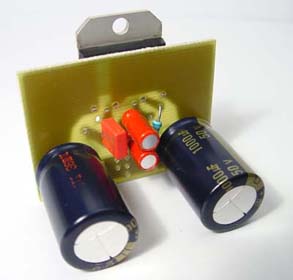
Figure 2.1, topside of the PCB
|
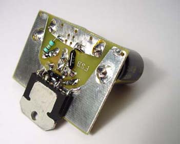
Figure 2.2, bottom side of the PCB
|
See figure 2.1 and 2.2 for an example of the parts you can use on the PCB's. This photo
is quite old so have a good look at the parts list too:
Parts needed for a single PCB:
- 1x LM3875T or LM3875TF
- 2x 22k
- 1x 680-ohm
- 1x 2,7-ohm
- 1x WIMA MKS2 0.1 uF 63V
- 2x Panasonic FC 1000uF 50V (or similar)
- 1x or 2x input capacitor
- 1x 1uF capacitor (>=100V)
Needed tools:
- Soldering iron
- Solder
- Desoldering pump or braid
- Pliers
- Cutter
- Multi-meter
- Wire stripper (optional)
See figure 2.3 for the Chill-amp II circuit:

Figure 2.3, Chill-amp II schematic
|
| 3. The hole labels |
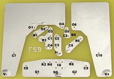
Figure 3.1, bottom side of the PCB with hole labels
In figure 3.1 the following holes are present:
O1, O2, O3, O4, O5 and O6: Opamp pins
R1-R2: 680-ohm resistor
R3-R4: 22k resistor
R5-R6: 1-ohm resistor
C1-C2, C4-C5: input capacitors (4.7 uF)
C3-C6: 0.22 uF capacitor
C7-C8, C9-C10: supply capacitors (1000 uF)
SO: speaker output (this hole is between C3 and O5, figure 3.1 is from a beta PCB)
SG: speaker output ground
V-: negative supply (-12V..-36V)
V+: positive supply (+12V..+36V)
G1, G2: supply grounds
I+: input signal (goes to the middle connector of the potmeter)
IG: input grounds
|
| 4. The soldering of the amplifier PCB |
Step 1, mounting the opamp on the PCB
- Cut off the last 6 mm of pin 1,3,5,7,9 and 11 of the opamp (after the bend of the pins). Pin 1 is the left pin if you look at the labeled side of the opamp.
- Cut off pins 2, 5, 6, 9 and 10. Do it very careful; don't touch the other pins! Don't make any mistakes in cutting: it will cost you an opamp! I remove the pins by moving the pins many times up and down. They will break off then! The cut off pins should not be larger than approx. 0.5 mm.
- Very gently bend pin 4 and 8 down to make them parallel with pin 3 and 7.
- Place the opamp on top of the bottom side of the PCB, through holes O1-O6. The text of the opamp is downwards (so you can't read it anymore after mounting). You'll have to bend pin 3 and 7 a bit to make the opamp fit. Don't use too much force. The label side of the opamp should be as close to the PCB as possible. Later on, you can glue them together if you want.
- Solder the six pins of the opamp. Ensure yourself that no short-circuits are made, especially not between pin 3 and 4 and pin 7 and 8! You can bend the pins that come out of the PCB on the other side a bit before soldering to reduce the chance of short circuits. It's probably the best to start soldering pin 1 and 11, while pressing the opamp to the PCB.
- On the other side of the PCB, the opamp pins will partly come out. Don't cut the pins 1 and 4 off, you can mount a small 1 uF capacitor here now! The end of the other pins can be cut off.
- Examine all of the soldered pins for good contact and no short-circuits.
Step 2, mounting the feedback resistor
- This is the hardest part of the build process. Take a 22k resistor and bend both wires down as close to the body of the resistor as possible. Cut the wires at about 7 mm from the resistor. Solder the resistor between pin 3 and pin 8 of the opamp (hole O2 and O5) and as close as possible! In my Chill-amp, the resistor makes contact with the solder side of the PCB and the side of the resistor makes contact with pin 4 and 7 (though not electrically!).
- Again, examine the soldering and watch out for short-circuits.
Step 3, mounting the input capacitors
- Now the input capacitors need to be mounted on the topside of the PCB.
- If you use a polar capacitor, mount the capacitor with the negative wire in hole C1 or C4 and the positive wire in C2 or C5.
- If you use two Blackgate N 4.7uF 50V capacitors, mount one in holes C1 and C2 and the second in holes C4 and C5. Rotate the second capacitor 180 degrees, to make the text different on the side. This is the super-E configuration for better sound!
- Cut off excess wire.
Step 4, mounting the supply capacitors
- The two 1000 uF Panasonic FC capacitors can now be soldered (through the holes C7, C8, C9 and C10). They will be placed on the topside of the PCB. It is very important to solder them in the right polarity! Electrolytic capacitors with a reversed polarity can be damaged or they can even explode! See figure 4.1 for the correct polarity of the capacitors. Ensure that the capacitor makes good contact with the PCB. If you want to, you can (carefully!) strip the labels of the capacitors for better sound.
- Cut off excess wire.
Figure 4.1, polarity of supply capacitors
Step 5, mount the zobel network
- Solder the 0.1 uF capacitor between C3 and C6. The capacitor is on the topside.
- Solder the 2.7-ohm resistor between R5 and R6, on the bottom side.
Step 6, mount the other resistors
- Solder a 680-ohm resistor between R1 and R2. The resistor is placed on the topside.
- Solder a 22k resistor between R3 and R4, on the bottom side.
Step 7, connect wires
- The last step is to connect wires to SO, SG, V-, V+, G1, G2, I+ and IG:
SO: speaker output (red)
SG: speaker output ground (black)
V-: negative supply (-38..-20V)
V+: positive supply ( 20..38)
G1, G2, IG: supply grounds and input ground
I+: input signal (connect to middle connector of the potmeter)
- Connect IG to the potmeter (or stepped attenuator) and from the potmeter to the
ground of the audio input connector. Also, connect a thick wire from the case to IG (for both PCB's!).
- I use 0.4mm 47 Labs OTA copper cable. Single core CAT5 wire will do fine too! I'd advise to
use two twisted CAT5 wires for the four supply wires, because the 0,4 mm wires can easily break
(and we really don't want that to happen with one of the sides of the supply!)
- Before connecting the supply wires, first check the supply (see chapter 5).
|
| 5. Chill-amp I supply PCB |
The supply PCB is only used for the Chill-amp I, but I left this in the manual for reference.
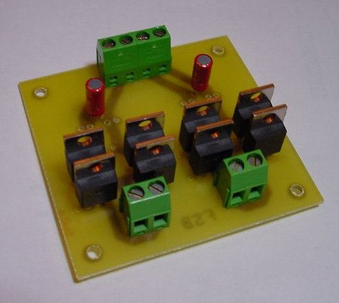
Figure 5.1, supply PCB
In figure 5.1, the supply PCB is shown. Eight MUR860 diodes are used for rectification. When you view the PCB from same side as in the figure, the diodes are mounted in the second and fourth holes (see picture closely). The print connectors should be mounted with the cable holes on the outside of the PCB. Optionally, capacitors can be placed in the middle of the PCB. Two BG 4.7 uF capacitors are shown in figure 1. They can be used to filter HF from the mains. Also, additional capacitance can be added (eg. 1000 uF or 2200 uF) to your taste.
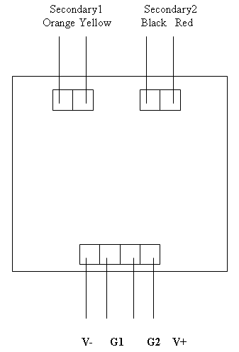
Figure 5.2, supply PCB connections
In figure 5.2, the supply PCB connections are shown (topside of PCB). The colors of the wires of the transformers I use are shown on top of the figure. If no wires are connected to the PCB and the diodes are mounted correctly, a (very) high resistance should be measured between Orange and Yellow and between Black and Red. Connect the transformers. Don't forget to add a fuse on the primary of the transformer! Be very careful with the mains; ensure that the electrical safety is undoubted! Measure V- and V+ to verify that the voltages are in the range (V+ should be 12V..36V and V- should be -36V..-12V).
For reference I have included the schematic of the supply:
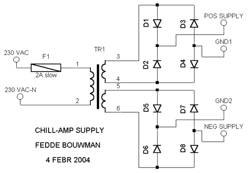
Figure 5.3, supply schematic
|
| 6. Chill-amp II supply |
The Chill-amp II makes use of a new supply circuit. It uses more transformers but less
diodes than the Chill-amp I. The idea is to create a faster and more transparent supply. See
figure 6.1 for the schematic. I currently use STPS20H100CT dual schottky diodes. They are
very practical, only two are necessary per channel! Building this supply should be
straightforward, but don't hesitate to contact me in case you have questions. Ensure very good
isolation at the mains side of the circuit for optimal safety!
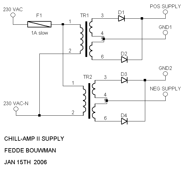
Figure 6.1, Chill-amp II supply schematic
|
| 7. The testing |
- Check all components and solder connections. Are all components tightly mounted to the PCB's?
- Measure if there are any short-circuits between the IC pins. Mount the opamp to the heatsink.
- In case of usage of the (non-shielded) LM3875T: measure the resistance between the heatsink and the negative supply. If there is a short-circuit, the chip is not isolated well!!!
- Check the electrical safety of the supply. Measure the supply voltages (without connecting the supply to the PCB). Is the voltage within the expected range? The measured voltage will be lower because no supply regulation capacitors are present! Turn-off the supply and connect the supply to the amplifier PCB. Don't forget that V-, G1, G2 and V+ in figure 3.1 are seen from the bottom of the amplifier PCB. Double check that the positive voltage is connected to V+ on the amplifer PCB, so connected to the positive side of the capacitor and connected to pin1 of the opamp. If you are confident that everything is connected properly, turn-on the supply (without speakers or source connected). Measure the output DC level. This should be well under 100 mV. Check if no significant voltage is present on the inputs.
- Connect a CD player or DAC and speakers to the amp! Now it is time for chilling :)
- Judge the sound quality only after the amp has been continously powered for a few days... The sound quite dramatically changes during break-in!!!
- And don't forget to send me an e-mail with your experiences!
|
Send me back to the Chill-amp II page please!
Show the other audio projects!!!
|
|
|